- 您现在的位置:买卖IC网 > Sheet目录2011 > MAX5890EGK+D (Maxim Integrated Products)IC DAC 14BIT LVDS 600MSPS 68-QFN
Detailed Description
Architecture
The MAX5890 high-performance, 14-bit, current-steer-
ing DAC (see the Functional Diagram) operates with
DAC update rates up to 600Msps. The current-steering
array generates differential full-scale currents in the
2mA to 20mA range. An internal current-switching net-
work, in combination with external 50
termination
resistors, converts the differential output currents into a
differential output voltage with a 0.1V to 1V peak-to-
peak output voltage range. The analog outputs have a
-1.0V to +1.1V voltage compliance. For applications
requiring high dynamic performance, use the differen-
tial output configuration and limit the output voltage
swing to ±0.5V at each output. An integrated 1.2V
bandgap reference, control amplifier, and user-selec-
table external resistor determine the data converter’s
full-scale output range.
Reference Architecture and Operation
The MAX5890 operates with the internal 1.2V bandgap
reference or an external reference voltage source.
REFIO serves as the input for an external, low-imped-
ance reference source or as a reference output when
the DAC operates in internal reference mode. For sta-
ble operation with the internal reference, bypass REFIO
to AGND with a 0.1F capacitor. The REFIO output
resistance is 10k
. Buffer REFIO with a high-input-
impedance amplifier when using it as a reference
source for external circuitry.
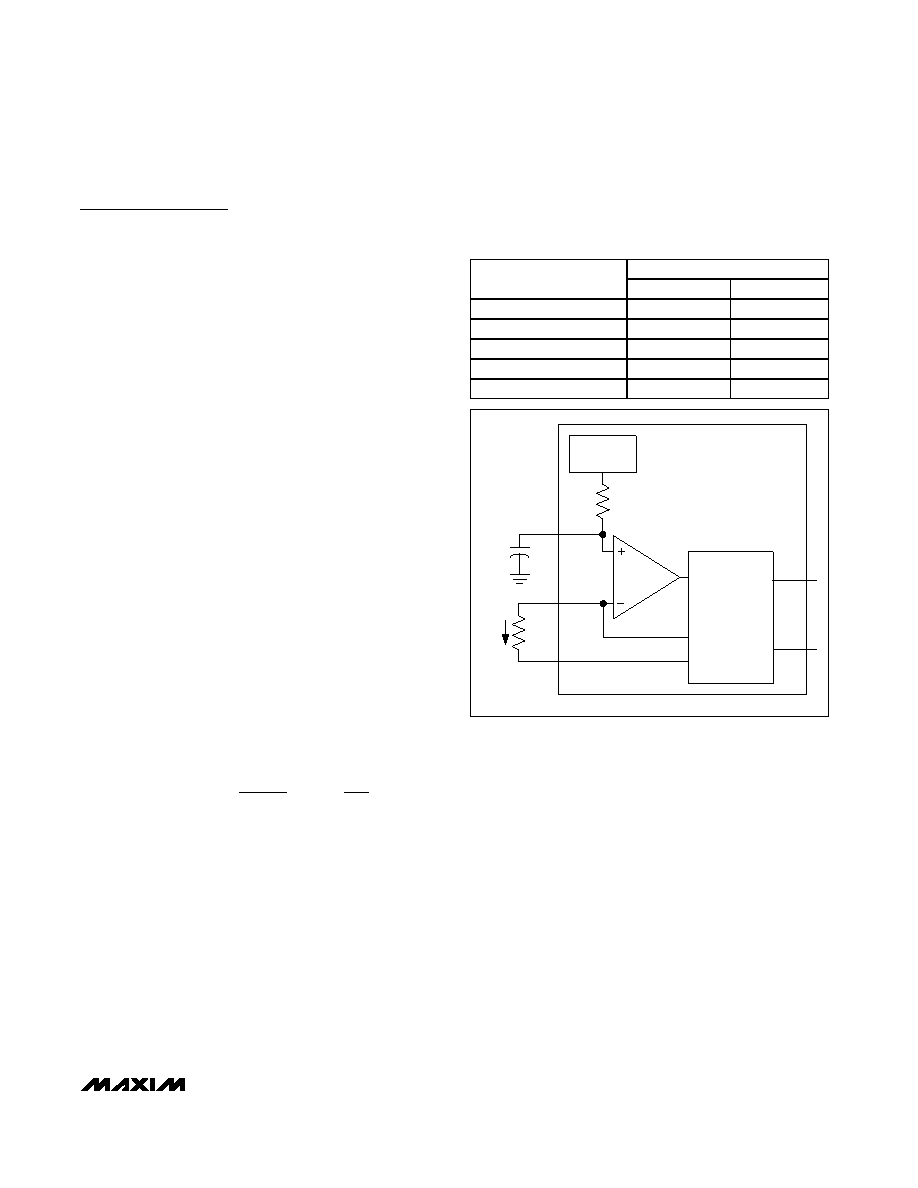
The MAX5890’s reference circuit (Figure 1) employs a
control amplifier to regulate the full-scale current,
IOUTFS, for the differential current outputs of the DAC.
Calculate the output current as follows:
where IOUTFS is the full-scale output current of the
DAC. RSET (located between FSADJ and DACREF)
determines the amplifier’s full-scale output current for
the DAC. See Table 1 for a matrix of different IOUTFS
and RSET selections.
Analog Outputs (OUTP, OUTN)
The complementary current outputs (OUTP, OUTN) can
be connected in a single-ended or differential configu-
ration. A load resistor converts these two output cur-
rents into complementary single-ended output
voltages. A transformer or a differential amplifier con-
verts the differential voltage existing between OUTP
and OUTN to a single-ended voltage. When not using a
transformer, terminate each output with a 25
resistor
to ground and a 50
resistor between the outputs.
To generate a single-ended output, select OUTP as the
output and connect OUTN to AGND. Figure 2 shows a
simplified diagram of the internal output structure of the
MAX5890.
I
V
R
OUTFS
REFIO
SET
=×
×
32
1
2
14
MAX5890
14-Bit, 600Msps, High-Dynamic-Performance
DAC with LVDS Inputs
_______________________________________________________________________________________
9
RSET (
)
FULL-SCALE CURRENT
IOUTFS (mA)
CALCULATED
1% EIA STD
2
19.2k
19.1k
5
7.68k
7.5k
10
3.84k
3.83k
15
2.56k
2.55k
20
1.92k
1.91k
Table 1. IOUTFS and RSET Selection Matrix
Based on a Typical 1.200V Reference
Voltage
OUTP
OUTN
1.2V
REFERENCE
CURRENT-SOURCE
ARRAY DAC
REFIO
FSADJ
RSET
IREF
10k
DACREF
0.1
F
IREF = VREFIO / RSET
Figure 1. Reference Architecture, Internal Reference
Configuration
发布紧急采购,3分钟左右您将得到回复。
相关PDF资料
MAX5891EGK+D
IC DAC 16BIT LVDS 600MSPS 68-QFN
MAX5893EGK+D
IC DAC 12BIT DUAL 500MSPS 68-QFN
MAX5894EGK+D
IC DAC 14BIT DUAL 500MSPS 68-QFN
MAX5895EGK+D
IC DAC 16BIT 500MSPS DUAL 68-QFN
MAX5898EGK+D
IC DAC 16BIT DUAL 500MSPS 68-QFN
MAX6900ETT+T
IC RTC I2C COMPAT 6-TDFN
MAX6902ETA+T
IC RTC SPI COMPAT 8-TDFN
MAX7375AXR604+T
IC OSC SILICON SC70-3
相关代理商/技术参数
MAX5890EGK+TD
功能描述:数模转换器- DAC 14-Bit 600Msps DAC RoHS:否 制造商:Texas Instruments 转换器数量:1 DAC 输出端数量:1 转换速率:2 MSPs 分辨率:16 bit 接口类型:QSPI, SPI, Serial (3-Wire, Microwire) 稳定时间:1 us 最大工作温度:+ 85 C 安装风格:SMD/SMT 封装 / 箱体:SOIC-14 封装:Tube
MAX5890EGK-D
功能描述:数模转换器- DAC RoHS:否 制造商:Texas Instruments 转换器数量:1 DAC 输出端数量:1 转换速率:2 MSPs 分辨率:16 bit 接口类型:QSPI, SPI, Serial (3-Wire, Microwire) 稳定时间:1 us 最大工作温度:+ 85 C 安装风格:SMD/SMT 封装 / 箱体:SOIC-14 封装:Tube
MAX5890EGK-TD
功能描述:数模转换器- DAC RoHS:否 制造商:Texas Instruments 转换器数量:1 DAC 输出端数量:1 转换速率:2 MSPs 分辨率:16 bit 接口类型:QSPI, SPI, Serial (3-Wire, Microwire) 稳定时间:1 us 最大工作温度:+ 85 C 安装风格:SMD/SMT 封装 / 箱体:SOIC-14 封装:Tube
MAX5890EVKIT#
功能描述:数模转换器- DAC RoHS:否 制造商:Texas Instruments 转换器数量:1 DAC 输出端数量:1 转换速率:2 MSPs 分辨率:16 bit 接口类型:QSPI, SPI, Serial (3-Wire, Microwire) 稳定时间:1 us 最大工作温度:+ 85 C 安装风格:SMD/SMT 封装 / 箱体:SOIC-14 封装:Tube
MAX5890EVKIT-W
制造商:Maxim Integrated Products 功能描述:- Bulk
MAX5891EGK
制造商:Rochester Electronics LLC 功能描述: 制造商:Maxim Integrated Products 功能描述:
MAX5891EGK+D
功能描述:数模转换器- DAC 16-Bit 600Msps DAC RoHS:否 制造商:Texas Instruments 转换器数量:1 DAC 输出端数量:1 转换速率:2 MSPs 分辨率:16 bit 接口类型:QSPI, SPI, Serial (3-Wire, Microwire) 稳定时间:1 us 最大工作温度:+ 85 C 安装风格:SMD/SMT 封装 / 箱体:SOIC-14 封装:Tube
MAX5891EGK+TD
功能描述:数模转换器- DAC 16-Bit 600Msps DAC RoHS:否 制造商:Texas Instruments 转换器数量:1 DAC 输出端数量:1 转换速率:2 MSPs 分辨率:16 bit 接口类型:QSPI, SPI, Serial (3-Wire, Microwire) 稳定时间:1 us 最大工作温度:+ 85 C 安装风格:SMD/SMT 封装 / 箱体:SOIC-14 封装:Tube